


Grosfontae is progressively preparing ultra violet photolithography for the next generation of chips.
Last year, separated from AMD chip manufacturing plant Globalfoundries (GlobalFoundries) has issued a statement, said AMD dacentrurus (Ryzen) and Epyc processor, and every kind of Radeon GPU, is by its exclusive oem. Now, with the maturity of the 14nm LPP process, grosfonde put the long-term goal on the Fab 8 manufacturing plant in northern New York. According to the company's Roadmap, the 7 nanometer Leading Performance process (7LP) will be the core of Grover's sprint to the next limit, and eventually it will be used in the manufacture of large scale semiconductor products using extreme ultraviolet lithography (EUV).

Although the semiconductor industry has been thinking about EUV technology for many years, the challenges in practical applications have not been delayed by the industry.
At present, there is only one ASML company on the market, and a company provides equipment in its exploration. Therefore, the fate of its technology depends on whether ASML can overcome the interference caused by the time limit between ultraviolet and X ray.
Unlike the argon fluoride excimer laser used in the current 193-mm immersion lithography tool, extreme ultraviolet scanning must rely on a completely new way to use the electromagnetic energy required for the next generation of technology on silicon wafer.
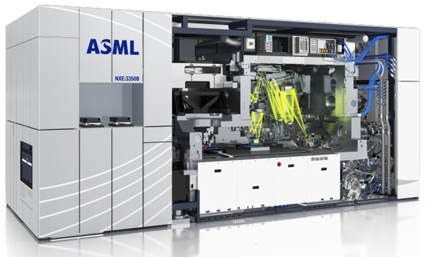
ASML extreme ultraviolet lithography scanner
It is reported that grove will redistribute the inside of the plant, and convert the molten tin droplet into high-energy plasma by laser pulse, and the wavelength of light generated is only 13.5 nm.
The traditional technology uses the refracting lens made of glass, but it has a great influence on the performance of light. EUV scanners must guide this valuable energy source, and let it pass through the mirror smoothly to the wafer, which needs to be realized in hard vacuum environment.
Even so, the light efficiency of the EUV scanner is still quite low. Even if the power of the light source has 250W, only about 2% on the surface of the wafer. Unfortunately, until the end of last year, ASML had not been able to cross the 250W milestone.
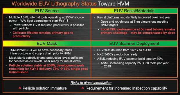
Some of the challenges EUV faces in mass production
Another big challenge for the EUV process is to find the right thin film. This transparent protective layer prevents debris in the production process from immersing in the mask, but it is still a difficult challenge at present.
Even under clean conditions, a protective shell is needed to cover the wafer, and the vacuum environment of the EUV device itself is guaranteed. Because tiny fragments still remain on the EUV network, and if there is a lack of film protection, debris may remain on the finished chip.
Like other EUV lasers, the film absorbs some light energy and reduces the amount of light that eventually reaches the wafer. The current EUV film material can transfer about 78% of the energy from the scanner to the wafer.
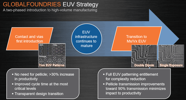
Glorfontae's EUV strategy
For grolfonder, it needs to break through at least 88% of the transmission efficiency before mass production. The good news is that Tom Caulfield, the chief technical officer of glorfontae, is optimistic about the prospects for EUV.
He believes that this technology will not affect the production of 7-nm chips. For a factory that can't stop every day, they will not step in before technology matures.
In the short term, EUV will not be the protagonist of the chip manufacturing. In glorfonde's 7-nm process, EUV will use only two places - the contacts and the vias.
