[scheme introduction]
In some industrial applications, often need to send commands to control local remote display characters, pictures and Chinese characters and other information, which requires an intelligent display terminal, can be used as industrial control, intelligent instrument and display terminal. In order to achieve quick response, the smart LCD terminal is usually designed with a high-performance M3/M4/A8/DSP processor, and can be equipped with touch screen module. The design of the intelligent liquid crystal display terminal uses STM32F103ZET6 as the main controller M3 core board 64M RAM, used to improve the system operation speed, and the capacity of 1G NAND FLASH, used to store pre design pictures, all kinds of graphics and Chinese characters ASCII code base, and an integrated RS232/RS485/USB interface according to the actual needs. In order to facilitate the installation of LCD panel on the control cabinet, the use of universal 24V power supply. The core processor and various peripherals are used in the design of the 3.3V power supply, the current consumption is expected to more than 500mA (up to 630mA current consumption of complex graphics processing by testing, in order to keep the design margin), more than 2 times, with an output voltage of 3.3V, voltage regulator chip TPS54331 output current up to 2A the. It is a 3.5V to 28V input 3A/570kHz Eco-mode buck converter, cost-effective, high temperature: -40 degrees ~150 degrees, can meet the industrial level equipment requirements. Here is the power design scheme implemented using the TI WEBENCH platform.
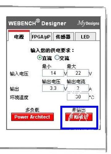
Input voltage: 24V; output voltage: 3.3V; output current: maximum 2A; operating temperature: set to 40 degrees centigrade. The design steps are as follows:
[scheme design]
(1) click start design
Because only one power source is available in the program, it's OK to just click on the red font [start design]. As shown:
This will load a FLASH login screen, which takes about 1 minutes, and goes into a default design interface:
As shown:
(2) set the input parameters and click the green button [recalculate], as shown in fig.:
Here, select [DC], DC input, minimum = maximum =24V, output voltage: 3.3V, output current: 2A, do not forget the temperature: 40 degrees centigrade. When these parameters are entered correctly, click on the recalculation to create a new design interface. As shown:
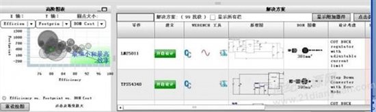
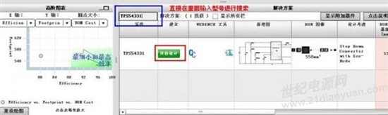
Because this design already has the physical design, therefore the chip already selected TPS54331, but here does not have, how then does? TI in this design link, increased search function, very practical Oh. As follows: we enter in: TPS54331, the system will automatically filter out the chip program:
(3) open the TPS54331 design proposal
In the above figure, click the green button [open the design], the system will automatically generate a TPS54331 chip power solutions, generated program interface as shown below:
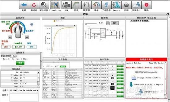
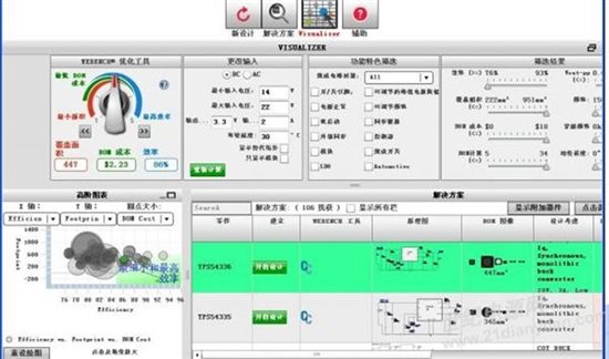
The content of the final design of the interface is very rich, you can see optimization options has been on the left show, here we do not have the time, the choice of TPS54331 is considered from the aspects of price, efficiency and current parameters etc.. If you redesign the flowers of a new program, you can make a choice among items such as minimum BOM cost [maximum efficiency] [coverage area], etc.. In the lower left corner of the interface, the generated technical scheme can be named and saved. Here, the program interface is divided into six windows, namely, [schematic] [work value] [material list] [optimization tool] [your entire design]. There are three charts in the chart area, as shown in the figure:
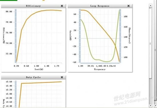
Respectively, efficiency, frequency response and duty cycle diagram.
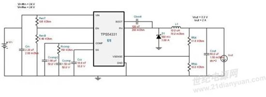
The schematic diagram of the design is as follows:
It can be exported through the EXPORT above the program interface, as shown in fig.:
WEBENCH supports the current mainstream PCB software tools, later introduced.
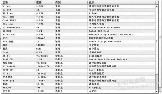
[work value] screenshot as follows: the information here is very large, the previous parameters can be explained by the following instructions, here no longer explain one by one.
Click on [material list] interface, the system will be the entire screen display, here you can list the output EXCEL form, easy access, you can see here BOM cost 3.7 U.S. dollars. WEBENCH each part gives detailed information, including the manufacturer, part number, quantity, price, property, covering an area of 3D, the effect of the top view, if you don't have a component, click on the green button can choose alternative [parts]
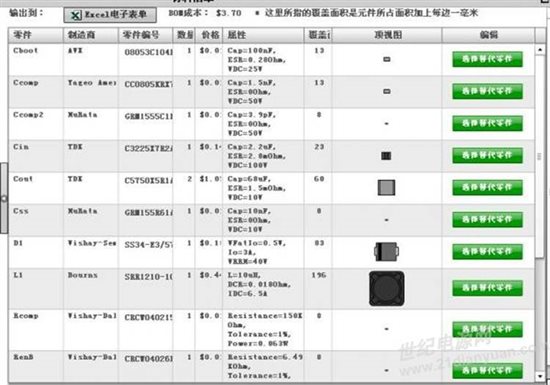
Here, I use a F104R type type inductor, which is also used in practice, which is usually not cheap.
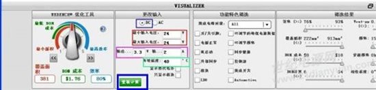
After you click the optimization options in the upper right corner of the interface, the system will give you some diagrams: Here's the diagram:
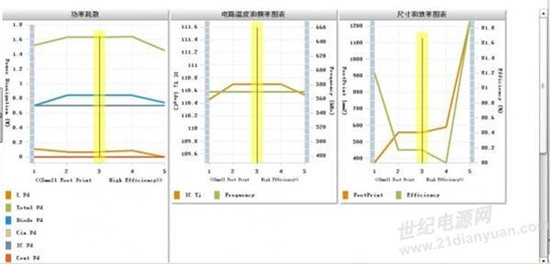
These three charts are power dissipation, circuit temperature and frequency, size, and efficiency diagrams. Through these diagrams, you can learn more about the various parameters of the TPS54331 chip scheme.
(4) generate design report and export schematic diagram
In the lower right corner of the entire chip program [your entire design], you can print design reports, export schematics. As shown:
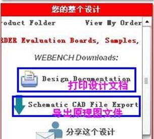
Click on the above [Design Documentation] can generate design reports, click [Schematic CAD File Export] you can export schematic.
The design report presented in PDF format, the overall description, by the scheme of circuit principle diagram, electrical materials, graphics, numerical and design input parameters and so on, through the design report, can a detailed analysis of the design of power supply scheme.
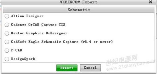
Click on the export schematic after the interface appears as below:
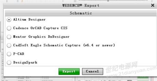
Here I'm accustomed to using Altium Designer, so choose the first option, wait a few seconds later, the following figure will appear:
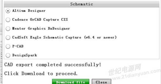
The prompt message is: the export successfully completed, you can click on the green button [Download file] to download. Click the download button, the following interface appears, find a suitable path, click OK to save it
Compressed files, which contain more content, screenshots as follows:
This tool is the reference time in the United States based on the time, so the design date of the above time than domestic similar day, inside the archive, the most important is the principle map file, the other can not, after opening with AD, as shown below: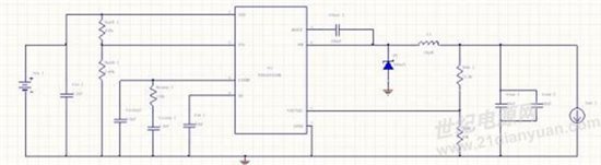
The graph is large, the format is irregular, and this has to be modified by itself. The new design should pay attention to this point!
(5) summary
It's easy to use the tool to design the power section. It usually takes a few minutes to a few tens of minutes to get a framework and report, and it's easy to make changes. If you find the right chip from TI's official website or power samples, at least half a day to get it. Through the design report, you can get all the information about the chip program:
The scheme adopts TPS54331DR chip, adopts BUCK topological structure, BOM costs 3.7 US dollars, according to the present price approximately: 23 yuan. Among them, TPS54331DR 0.75 U. s.dollars, about 5 yuan. Total power: 1.63W, area size 558MM2, BOM quantity 15. You can get it by following chart,
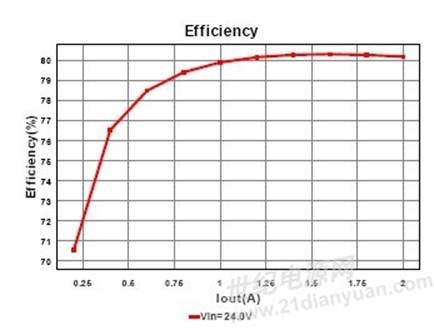
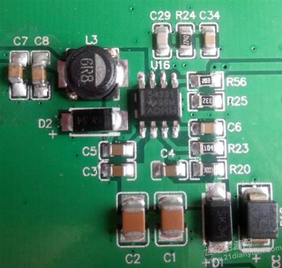
When the output current is 500mA, the efficiency can reach more than 75%. When the maximum 630mA is used, the efficiency is close to 78%. This efficiency is much better than the general AMS117 scheme. The following is the design of physical pictures: